exercise 09 :: Calculation of surface states, work function and STM
In the present exercise we construct a finite thick film of fcc Cu with (001) surface and calculate electronic properties as well as work function and STM image.
TASK 01
Consider fcc Cu as in exercise 05 assuming lattice constant of 3.597 Angstrom, and pseudopotential Cu.pbe-dn-kjpaw_psl.1.0.0.UPF with the energy cutoff ecutoff = 45 and for the kinetic energy cutoff for charge density and potential ecutrho = 240. Construct a finite thick slab containing 3 unit cells (UC) of fcc Cu and 3 empty unit cells to model a vacuum separating the Cu unit cells in (001) direction forming a surface. Analyze the following input and perform scf calculations
 &control
     title = 'fcc Cu (001) surface model via 3UC slab'
     calculation = 'scf'
     restart_mode = 'from_scratch',
     pseudo_dir = './',
     outdir = './tmp',
     prefix = 'cu'
     tprnfor = .true.
     tstress = .true.
 /
 &system
     ibrav = 0, nat = 7, ntyp = 1,
     ecutwfc = 45, ecutrho = 240, occupations = 'smearing',
     smearing = 'marzari-vanderbilt', degauss = 0.01
 /
 &electrons
     startingpot = 'file'
     conv_thr = 1.D-7
     diagonalization = 'david'
     mixing_beta = 0.7
 /
 ATOMIC_SPECIES
     Cu  63.546 Cu.pbe-dn-kjpaw_psl.1.0.0.UPF
 ATOMIC_POSITIONS crystal
     Cu 0.0 0.0 0.0
     Cu 0.5 0.5 0.08333333
     Cu 0.0 0.0 0.16666666
     Cu 0.5 0.5 0.25
     Cu 0.0 0.0 0.33333333
     Cu 0.5 0.5 0.41666666
     Cu 0.0 0.0 0.5
 K_POINTS (automatic)
    10 10 1   0 0 0
 CELL_PARAMETERS angstrom
    2.543463  0.0  0.0
    0.0  2.543463  0.0
    0.0  0.0  21.582
and bands calculations along the projected high symmetry points in 2d Brillouin zone connecting the following points:
0.5  0.5  0.0  28  !M
0.0  0.0  0.0  20  !G
0.5  0.0  0.0  20  !X
0.5  0.5  0.0  1   !M
Calculate projected density of states (PDOS) to distinguish between the states originating from the surface Cu atoms and those from the bulk.

TASK 02
Calculate work function for the fcc Cu slab. Use electronic density and wavefunction from the nscf calculation of PDOS and calculate potential using pp.x program with the following input
&inputPP
   outdir='./tmp',
   prefix='cu'
   plot_num=11
   filplot='fcc_Cu_slab.potential'
/
For the input variables refer to input description. To average the potential in xy planes use average.x program with the following input
1
fcc_Cu_slab.potential
1.D0
400
3
2.67
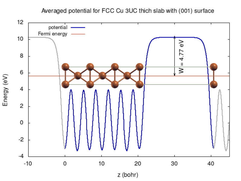
The averaged potential in shown in the figure below with a slab ball-stick structure overlay. The work function is a difference between the Fermi energy and potential value in the vacuum region.

TASK 03
Calculate scanning tunneling microscopy image in Tersoff & Hamann approximation for bias voltage of 1 eV and distance of 2 Angstroms from the surface. For this purpose use pp.x program with the following input file
 &inputpp
    prefix  = 'cu'
    outdir='./tmp',
    filplot = 'stm_bias_1eV'
    sample_bias = 0.0735d0,
    plot_num = 5
 /
 &plot
   nfile=1
   filepp(1)='stm_bias_1eV'
   weight(1)=1.0
   iflag=2
   output_format=3
   e1(1)=1.0, e1(2)=0.0,  e1(3)=0.0
   e2(1)=0.0, e2(2)=1.0,  e2(3)=0.0
   x0(1)=0.0, x0(2)=0.0,  x0(3)=5.0231
   nx=120, ny=120
   fileout = 'stm_bias_1eV_top_z2A.xsf'
 /
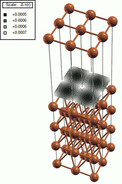
The result is stored in xsf file can be plotted using xcrysden (click Tools --> Data grid), see figure below.

Links:
Construction of slabs with particular surfaces using VESTA see Tasci’s guide.
Martin Gmitra :: martin.gmitra@upjs.sk
 This work is licensed under a Creative Commons Attribution 4.0 International License.